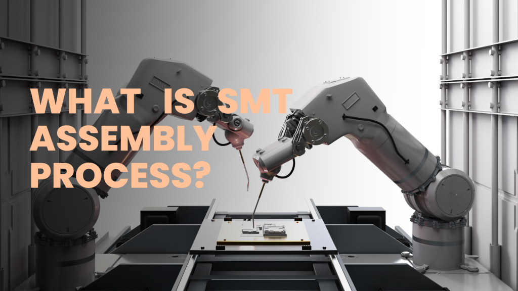
What is surface mount Technology (SMT) process? the full form for SMT in electronics is Surface mount Technology. Surface mount technology (SMT) process is the process where electronics devices are mounted on to the surface of a printed circuit board. This process very important in Manufacturing electronics and is one of the technologies used by many electronics manufacturer. This SMT process is done by a surface mount technology component placement system also called as pick and place machine.
This is done with high precision and high-speed placing the surface mount devices (SMD) on to the Printed circuit Boards (PCB). Surface Mount Technology (SMT) has revolutionized electronics manufacturing, enabling smaller, more efficient, and cost-effective products. In a growing word of Electronics SMT also known as surface mount technology is very important is a very important and adopted widely by many electronics manufacturers.
Table of Contents
What are the steps involved in Surface Mount Assembly or SMT process?
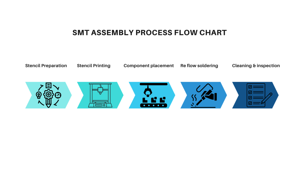
Surface Mount Technology (SMT) is the backbone of modern electronics manufacturing. The major SMT process involves 5 major steps They are
- Stencil Preparation
- Stencil Printing
- Component placement
- Re flow soldering
- Cleaning and inspection
These steps are often followed by additional processes such as SMT inspection and testing, cleaning, conformal coating, and final assembly, depending on the specific product requirements. Let’s dive deep into each stage of SMT process,
Stencil Preparation:
What is stencil in electronics? It’s a thin sheet of metal with laser cut apertures, which acts a template for depositing solder paste onto the PCB. A well-prepared stencil is essential for consistent solder paste deposition, ensuring optimal component placement and subsequent soldering.
At first a digital representation of the PCB’s solder pad layout will be made and laser cutting machine programmed with the high precision is used to create the desired aperture with exceptional accuracy.
The stencil is the back bone that decided the overall quality and reliability of the other subsequent steps in SMT process.
Stencil printing or solder paste application:
Stencil printing is the initial step in the SMT process. It’s where the blueprint for the electronic circuit starts to take shape. It involves depositing solder paste onto a printed circuit board (PCB) in preparation for component placement.
How is stencil printing is done?
- Stencil aligning:
A stencil, which is a thin metal sheet with laser-cut apertures, is aligned with the PCB. The apertures correspond to the locations of the solder pads on the PCB.
The stencil is securely clamped onto the PCB.
- Solder Paste Application:
- Solder paste, a mixture of metal alloy powder and flux, is applied to the stencil.
- A squeegee is moved across the stencil, forcing the solder paste through the apertures and onto the PCB’s solder pads. The amount of solder paste deposited is determined by factors such as stencil thickness, aperture size, and squeegee pressure.
- Stencil Removal:
- Once the solder paste is deposited, the stencil is carefully removed from the PCB.
After stencil printing the PCB’s goes for inspection to asses the quality of printing.
Component placement:
Its nothing but placing the electronics components on to the solder paste deposited on the Printed circuit board (PCB). This is done with high precision and speed. This method is more often done by automated pick and place machine. The components are picked from feeder and accurately placing them on the designated pads and will inspect for defects.
There are different types of component placement like pick and place, chip shooter and tape and reel feeder. The component placement, precision and speed affect the quality and efficiency of the final product.
Reflow soldering:
This is the stage where the components are permanently bonded on to the PCB. After all of the above process the PCB containing the solder paste, components and others are subjected to controlled heat. This controlled heat will help the solder paste melt and solidify to make electrical connections between the components and the board. This is done in a controlled heat cause the excess heat can cause damage to the electrical components.
Cleaning and inspection:
In this step the reliability and longevity of the electronics product is ensured by cleaning and inspection in an SMT process.
When it comes to cleaning the primary goal is to remove flux residues, which are chemical compounds left behind after the reflow soldering process. These residues can attract moisture, leading to corrosion and electrical short circuits.
PCB Inspection is to ensure and guarantee the quality of the assembled PCB. It involves a series of checks to identify defects and ensure the over all quality of the assembled product.
The various methods used by electronic manufacturing services are
1) Visual inspection: A manual process where operators examine the PCB for obvious defects like missing components, incorrect placement, solder bridges, or open circuits.
2) Automated Optical Inspection (AOI): This uses cameras and image processing to detect defects such as missing components, incorrect component orientation, solder defects, and component placement errors.
3) X-ray inspection (AXI): This non-destructive technique can identify hidden defects like voids, solder bridges, and component cracks.
4) In-circuit testing (ICT): This method verifies the connectivity between components on the PCB.
These are the various steps in a SMT process. Each ad every stem in SMT process is very important and decides the overall quality of the products. Keeping this in mind electronics manufacturers are aware and undergoes various optimization and maintains quality in each an every step of the SMT process.
SMT assembly process flow chart

Advantages of surface mounting Technology
SMT has revolutionized electronics manufacturing due to its numerous benefits:
Miniaturization and Compactness
- Smaller components: SMT components are significantly smaller than through-hole components, allowing for denser circuit board designs.
- Thinner PCBs: SMT enables the creation of thinner and lighter electronic devices.
Increased Efficiency and Production Speed
- Automation: Most SMT processes are highly automated, leading to faster production times and reduced labor costs.
- Reduced assembly time: The placement of components is quicker compared to through-hole technology.
Improved Reliability and Performance
- Stronger joints: SMT typically results in stronger and more reliable solder joints.
- Better electrical performance: Shorter lead lengths and reduced inductance lead to improved signal integrity.
- Enhanced thermal management: Better heat dissipation due to component placement.
Cost-Effective
- Reduced material costs: Less material is required for SMT PCBs compared to through-hole boards.
- Lower labor costs: Automation and faster production times contribute to lower labor costs.
Design Flexibility
- Double-sided PCBs: SMT allows for components to be placed on both sides of the PCB.
- Complex designs: SMT can accommodate intricate and complex circuit board designs.
Environmental Benefits
- Reduced waste: Less material is used in the manufacturing process.
SMT assembly technology is one of the preferred and known method for assembling electronic components in terms of size, speed, quality and cost efficient.
Surface Mount Technology (SMT) has revolutionized electronics manufacturing by enabling the production of smaller, more efficient, and cost-effective products. The process, involving stencil preparation, solder paste application, component placement, reflow soldering, and cleaning, is highly automated for speed and precision. With its ability to miniaturize devices, increase production efficiency, enhance reliability, and reduce costs, SMT has become the industry standard for assembling electronic components. As technology continues to advance, SMT will remain a crucial cornerstone in the manufacturing of electronic products
Looking for a reliable and efficient PCB assembly partner?
We are one of the best electronics manufacturing services companies in Bangalore with high quality PCB assembly facility. Our team of experts is here to turn your vision into reality.
Contact us today for a free consultation and see how our SMT assembly process can bring your ideas to reality.