Our life is so much dependent on electronics from the smartphones we use to cars we travel. Ever wonder how these complex products are getting manufactured?
Let’s take a look at what we are going to cover in the blog.
Table of Contents
What Is electronics manufacturing process?
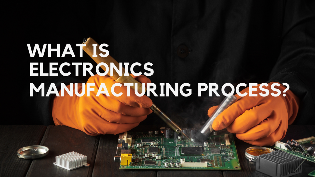
Electronics manufacturing process is the method of manufacturing an electronics product from concept to a usable electronic product. Electronics manufacturing consist of different processes starting from Design, prototyping, component sourcing, PCB assembling, Final product assembly, Quality control and shipping.
Electronics manufacturers invest in equipment and skills to provide high quality manufacturing services to OEMs and electronics brands. They handle all of these complex steps in electronics manufacturing process.
Electronics manufacturers serve as subcontractors for OEMs, handling their manufacturing needs.By outsourcing the OEMs have great advantage in terms of cost cutting and time and could focus more on important parts of the business.
Different steps involved in electronics manufacturing process
- BOM submission
- Design
- Component sourcing
- PCB assembly
- Box build or final product assembly
- Testing and inspection
- Packing and shipping
1) BOM submission: What is BOM? BOM or bill of material is nothing but a document which contains the list of components that is required to manufacture the product. It serves as a blue print for entire production process, ensuring the right components and procured, assembled and meet the desired specification asked by the customer.
This document should be submitted by OEMs to electronics manufacturer at first. Once the OEM submits the BOM to the manufacturing facility, the facility can review it, procure the necessary components, and begin the production process. However, there might be instances where the manufacturing facility might suggest modifications or alternatives to the BOM based on factors like availability, cost, or manufacturing constraints.
2) Design: The next step after BOM submission is designing. This is the crucial steps in manufacturing where the PCB layout and component placement design is decided here. This is where the BOM is translated in to physical design.
This step can be further breakdown into 4
- PCB Layout: The first step in PCB layout design involves creating a schematic diagram that visually represents the component interconnections specified in the BOM. Each component is assigned a PCB footprint defining its physical dimensions and pin arrangement. The layout engineer then connects these components using traces on the PCB, ensuring correct electrical signal flow.
- Component Placement: The placement of components on a PCB is influenced by various factors, including size, heat dissipation, and signal integrity. To ensure manufacturability and reliability, the layout engineer must adhere to design rules such as minimum clearances between components, trace widths, and via sizes. Additionally, components that generate significant heat should be placed in a way that allows for proper cooling.
- Verification and validation: To ensure the quality of the PCB design, various checks are performed, including design rule checks (DRC) to identify potential layout issues, electrical rule checks (ERC) to verify the absence of electrical errors, and signal integrity analysis through simulations to assess the quality of electrical signals on the PCB.
- Manufacturing data generation: The final PCB layout is converted into Gerber files, which are used by the PCB fabrication facility to manufacture the physical board. Additionally, drill files are generated to specify the location and size of the holes that need to be drilled in the PCB.
3) Component sourcing: After the designing process the next step is to source components. The components in the BOM needs to be sourced from reliable supplier. Because the components should be free from defects and good in terms of quality.
The component sourcing should be taken carefully because the suppliers should be not get disrupted by any sort of supply chain disruption.
4) PCB assembly: after designing and sourcing quality components from supplier the next step is to assemble the PCB. A PCB can be assembled through many ways. A PCB will be fabricated at first and then the components will assemble on it this is called PCB assembly. Surface mount technology (SMT) and Through hole technology (THT) are the most common technology used in assembling a PCB. The components are placed on to the board by automated machines and soldered.
5) Box build assembly or final product: The assembled PCB is the placed into an encloser which is used to house the PCB and other components to make it a final electronics product. This enclosure can be of any material it can be plastic, metal or other.
This is where the other components of the electronic product is connected such as monitor, display, buttons and others based on the design.
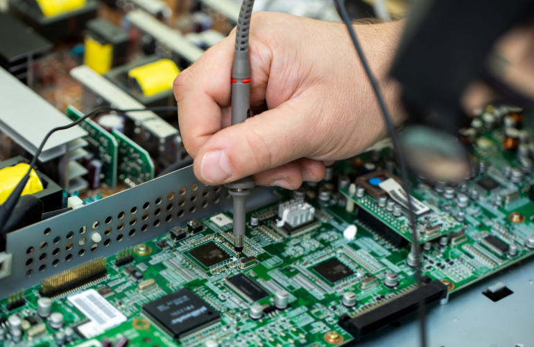
6) Testing and quality control: Testing after PCB assembly typically involves a series of inspections and functional checks to ensure the quality and reliability of the assembled board. This may include visual inspections for any physical defects or damage, functional tests to verify that all components are working as intended, and electrical tests to measure resistance, capacitance, and other electrical parameters. Additionally, specific tests may be conducted based on the board’s intended function, such as signal integrity testing for high-speed boards or environmental testing to assess the board’s performance under extreme conditions. These tests help identify any issues or defects early in the manufacturing process, allowing for corrective actions to be taken before the board is further integrated into the final product.
The different types of testing involved are:
- Visual Inspection: A manual or automated check for physical defects like scratches, cracks, or misaligned components.
- Functional Testing: Verifying that all components and circuits are working as designed. This may involve testing specific functions or simulating real-world conditions.
- Electrical Testing: Measuring electrical parameters like resistance, capacitance, and voltage to ensure they meet specifications.
- Signal Integrity Testing: Assessing the quality of electrical signals transmitted through the PCB, particularly important for high-speed applications.
- Power Integrity Testing: Evaluating the distribution of power on the PCB to ensure adequate supply and avoid voltage drops.
- Environmental Testing: Exposing the PCB to extreme conditions (e.g., temperature, humidity, vibration) to assess its durability and reliability.
- Thermal Imaging: Using infrared cameras to identify hot spots on the PCB, which can indicate potential overheating or design issues.
- X-Ray Inspection: Non-destructive testing method to detect internal defects like voids or cracks.
- In-Circuit Testing (ICT):: Automated testing of components and connections on the PCB using dedicated test fixtures.
- Functional Test Systems (FTS):: Automated systems that simulate real-world conditions and test the PCB’s overall functionality.
7)Packing and shipping: The electronics products are sometimes prone to damage by physical force or static energy. They need to be packed and shipped to customers. These products are shipped to wholesalers, distributor or directly to consumers.
Event after this manufacturing process they provide aftermarket services like repair and rework.
In conclusion, the electronics manufacturing process is a complex and intricate series of steps that involves everything from design and component sourcing to assembly and quality control. Understanding this process is crucial for businesses involved in the electronics industry.
If you’re looking for reliable and efficient electronics manufacturing services, we encourage you to contact us. Our team of experts can help you with every stage of the process, from initial design to final delivery.
Get fast and reliable Electronics Manufacturing Services
We are one of the best electronics manufacturing services companies located in Bangalore with high quality PCB assembly facility and Box build services. Our team of experts is here to help you with quality production services.
Contact us today for a Free consultation.


